General Description
The RT4730 is a highly integrated power soluction with Buck-Boost, and inverting charge pump to generate positive and negative output voltage. The negative output voltages can be adjusted from -0.6V to -4V with 100mV steps.
The positive output voltages can be adjusted from 2.8V to 4V with 100mV steps by SWIRE interface protocol. With its input voltage range of 2.9V to 5.2V, the RT4730 is optimized for products powered by single-cell battery and the output current up to 50mA.
Performance Sepcification Summary
Summary of the RT4730 Evaluation Board performance specificiaiton is provided in Table 1. The ambient temperature is 25°C.
Table 1. RT4730 Evaluation Board Performance Specification Summary
|
Specification
|
Test Conditions
|
Min
|
Typ
|
Max
|
Unit
|
|
Input Voltage Range
|
|
2.9
|
3.7
|
5.2
|
V
|
|
Quiescent Current
|
AVDDEN = high, SWIRE = high
|
200
|
400
|
500
|
µA
|
|
AVDDEN = high, SWIRE = low
|
100
|
200
|
300
|
µA
|
|
Shutdown Current
|
AVDDEN = low, SWIRE = low
|
--
|
0.01
|
2
|
µA
|
|
Output Current
|
|
50
|
--
|
--
|
mA
|
|
Default Output Voltage
|
AVDD = 3.3V OVDD = 3.3V OVSS = -3.3V
|
--
|
3.3
|
--
|
V
|
|
Operation Frequency
|
|
2.75
|
--
|
3.25
|
MHz
|
|
Output Ripple Voltage
|
ILOAD = 10mA
|
--
|
10
|
20
|
mVp-p
|
|
Output Voltage Accuracy
|
ILOAD = 0mA
|
-1
|
--
|
1
|
%
|
|
Line Regulation
|
VIN = 2.9V to 5.2V, ILOAD = 10mA
|
--
|
±1
|
--
|
mV
|
|
Load Regulation
|
ILOAD = 0mA to 10mA
|
--
|
±1
|
--
|
mV
|
Power-up & Measurement Procedure
1. Connect input power (2.9V < VIN < 5.2V) and input ground to VIN and GND test pins respectively.
2. Connect positive end and negative terminals of load to OVDD and OVSS and AVDD test pins respectively.
3. There is a 3-pin header “SWIRE” and “AVDD_EN” for enable control. To use a jumper at “H” option (upper side) to tie SWIRE test pin to input power VIN for enabling the device. Inversely, to use a jumper at “L” option to tie SWIRE test pin and ground GND for disabling the device.
4. Verify the output voltage (typically 6.6V) between OVDD and OVSS.
5. Connect an external load up to 50mA to the OVDD and OVSS and AVDD terminals and verify the output voltage and current.
OVDD and OVSS Output Voltage Setting
Set the negative output voltage with the Single Wire Protocal (SWIRE). Send the specified pulses to the header of SWIRE to program the OVDD and OVSS voltage. The output voltage is set by the following table:
SWIRE Setting
|
Pulse
|
Function Description
|
|
0
|
Default value: OVDD = 3.3V, OVSS = -3.3V
|
|
116
|
OVDD is turned on
|
|
117
|
VON/OVSS is turned on
|
|
118
|
OVDD is turned off
|
|
119
|
VON/OVSS is turned off
|
|
120
|
VON/OVSS discharge to GND, with slow slew rate then enter high impendance state
|
|
121
|
Soft-reset, clear all setting and back to default state
|
|
10-22
|
OVDD setting ( 2.8V to 4V)
|
|
58-92
|
OVSS setting (-4V to -0.6V)
|
|
Pulse
|
VOUT
|
OVDD
|
|
10
|
3.5
|
2.8
|
|
11
|
3.5
|
2.9
|
|
12
|
3.5
|
3
|
|
13
|
3.5
|
3.1
|
|
14
|
3.5
|
3.2
|
|
15
|
3.5
|
3.3
|
|
16
|
3.6
|
3.4
|
|
17
|
3.7
|
3.5
|
|
18
|
3.8
|
3.6
|
|
19
|
3.9
|
3.7
|
|
20
|
4
|
3.8
|
|
21
|
4.1
|
3.9
|
|
22
|
4.2
|
4
|
|
Pulse
|
VON
|
OVSS
|
Pulse
|
VON
|
OVSS
|
|
58
|
-4.1
|
-4
|
76
|
-2.3
|
-2.2
|
|
59
|
-4
|
-3.9
|
77
|
-2.2
|
-2.1
|
|
60
|
-3.9
|
-3.8
|
78
|
-2.1
|
-2
|
|
61
|
-3.8
|
-3.7
|
79
|
-2
|
-1.9
|
|
62
|
-3.7
|
-3.6
|
80
|
-1.9
|
-1.8
|
|
63
|
-3.6
|
-3.5
|
81
|
-1.8
|
-1.7
|
|
64
|
-3.5
|
-3.4
|
82
|
-1.7
|
-1.6
|
|
65
|
-3.4
|
-3.3
|
83
|
-1.6
|
-1.5
|
|
66
|
-3.3
|
-3.2
|
84
|
-1.5
|
-1.4
|
|
67
|
-3.2
|
-3.1
|
85
|
-1.4
|
-1.3
|
|
68
|
-3.1
|
-3
|
86
|
-1.3
|
-1.2
|
|
69
|
-3
|
-2.9
|
87
|
-1.2
|
-1.1
|
|
70
|
-2.9
|
-2.8
|
88
|
-1.1
|
-1
|
|
71
|
-2.8
|
-2.7
|
89
|
-1
|
-0.9
|
|
72
|
-2.7
|
-2.6
|
90
|
-0.9
|
-0.8
|
|
73
|
-2.6
|
-2.5
|
91
|
-0.8
|
-0.7
|
|
74
|
-2.5
|
-2.4
|
92
|
-0.7
|
-0.6
|
|
75
|
-2.4
|
-2.3
|
|
|
|
VOUT = MAX(AVDD, OVDD, |OVSS|) + 0.2V
Detailed Description of Hardware
Headers Description and Placement
Carefully inspect all the components used in the EVB according to the following Bill of Materials table, and then make sure all the components are undamaged and correctly installed. If there is any missing or damaged component, which may occur during transportation, please contact our distributors or e-mail us at evb_service@richtek.com.
Test Points
The EVB is provided with the test points and pin names listed in the table below.
|
Test point/
Pin name
|
Signal
|
Comment (expected waveforms or voltage levels on test points)
|
|
VIN
|
Input voltage
|
Power input. Support 2.9V to 5.2V input coltage. Must bypass with a suitable large ceramic capacitor at this pin.
|
|
SWIRE
|
Single wire protocal
|
Enable and OVDD and OVSS voltage setting.
|
|
AVDDEN
|
Single wire protocal
|
Enable AVDD voltage.
|
|
VON
|
Negative charge pump output
|
Negative charge pump output. It’s typically 3.3V.
|
|
GND
|
Ground
|
Ground.
|
|
VOUT
|
Buck-Boost voltage
|
Output voltage of Buck-Boost converter. It’s typically 3.5V (default setting).
|
|
OVDD
|
Positive terminal output
|
The output of a LDO. It is set at a typical value of 3.3V, It is set at a typical value of 3.3V and can be programmed through SWIRE
|
|
OVSS
|
Negative terminal output
|
The output of an inverting charge pump. It is set at a typical value of -3.3V and can be programmed through SWIRE
|
|
AVDD
|
Positive terminal output
|
Output voltage of boost converter. It is typically 3.3V.
|
|
C1P, C1N
|
Flying capacitor 1 positive and negative connection
|
Connect 1µF between C1P and C1N for inverting charge pump operation.
|
Bill of Materials
|
Reference
|
Qty
|
Part Number
|
Description
|
Package
|
Manufacture
|
|
U1
|
1
|
RT4730WSC
|
DC-DC Converter
|
WL-CSP-16B 2.34x2.34 (BSC)
|
RICHTEK
|
|
C1
|
1
|
C1608X5R1E475KT000E
|
4.7µF/25V/X5R
|
0603
|
TDK
|
|
C2
|
1
|
0603X105K250CT
|
1µF/25V/X5R
|
0603
|
WALSIN
|
|
C3, C5, C17
|
4
|
0603X106M6R3CT
|
10µF/6.3V/X5R
|
0603
|
WALSIN
|
|
C4, C6
|
2
|
0603X475K6R3CT
|
4.7µF/6.3V/X5R
|
0603
|
Murata
|
|
C7, C15
|
5
|
JMK107BBJ226MA-T
|
22µF/6.3V/X5R
|
0603
|
TAIYO YUDEN
|
|
C8
|
1
|
0603B104K500CT
|
0.1µF/50V/X5R
|
0603
|
WALSN
|
|
C9, C10, C11, C12, C13, C14, C16
|
8
|
NC
|
NC
|
0603
|
|
|
L1
|
1
|
1269AS-H-2R2M
|
2.2µH
|
2.5x2.0x1.0mm
|
Murata
|
|
L2
|
1
|
1269AS-H-2R2M=P2
|
2.2µH
|
2520
|
Murata
|
|
R1
|
1
|
WR06X000 PTL
|
0
|
0603
|
WALSIN
|
|
R2, R3, R6, R7, R8
|
5
|
NC
|
NC
|
0603
|
|
|
R4, R5
|
2
|
WR06X4701FTL
|
4.7k
|
0603
|
WALSIN
|
|
CP1, CP2
|
2
|
|
Short
|
0603
|
|
Typical Applications
EVB Schematic Diagram
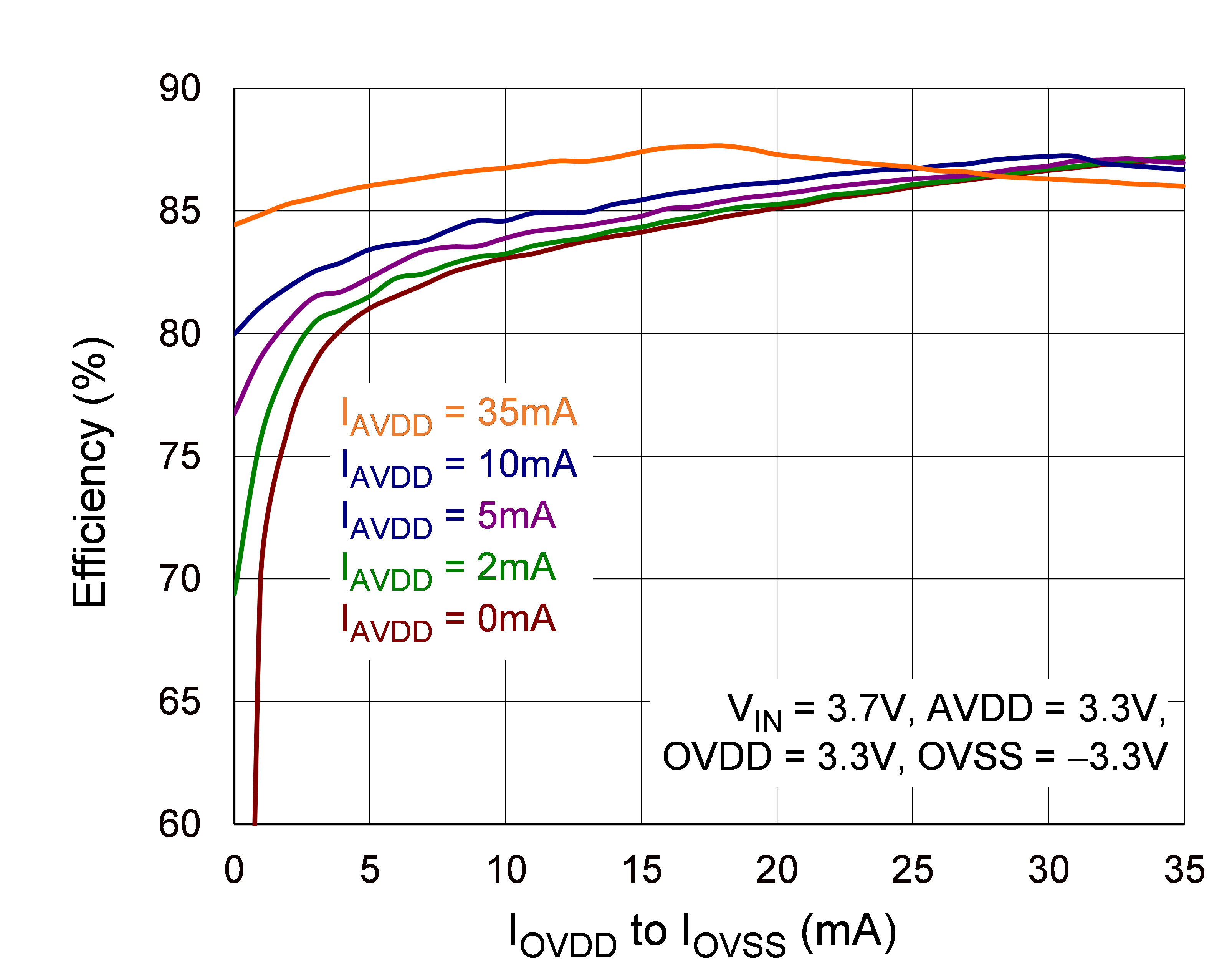
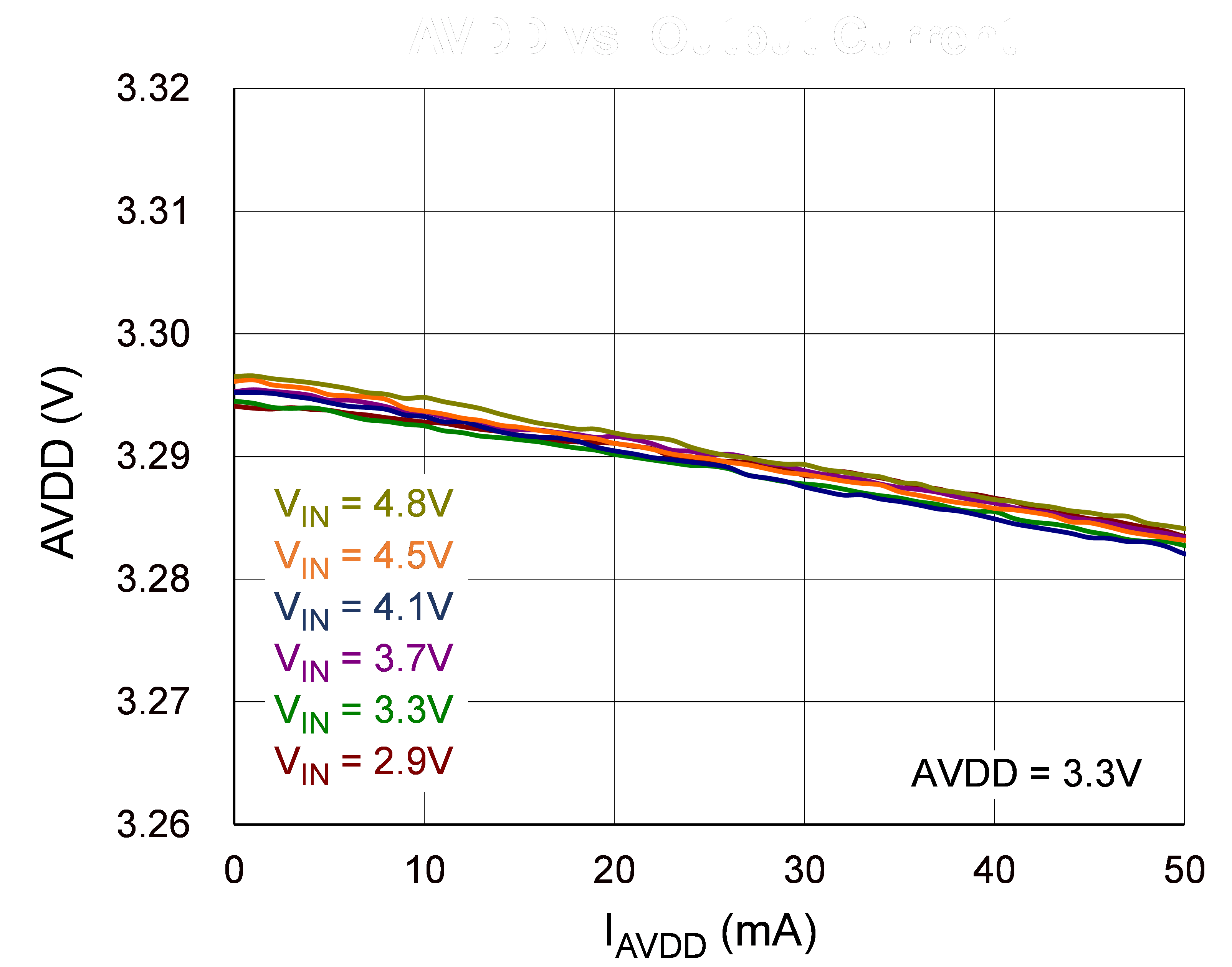
Measure Result
|
Efficiency vs. Output Current
|
AVDD vs. Output Current
|
|
|
|
|
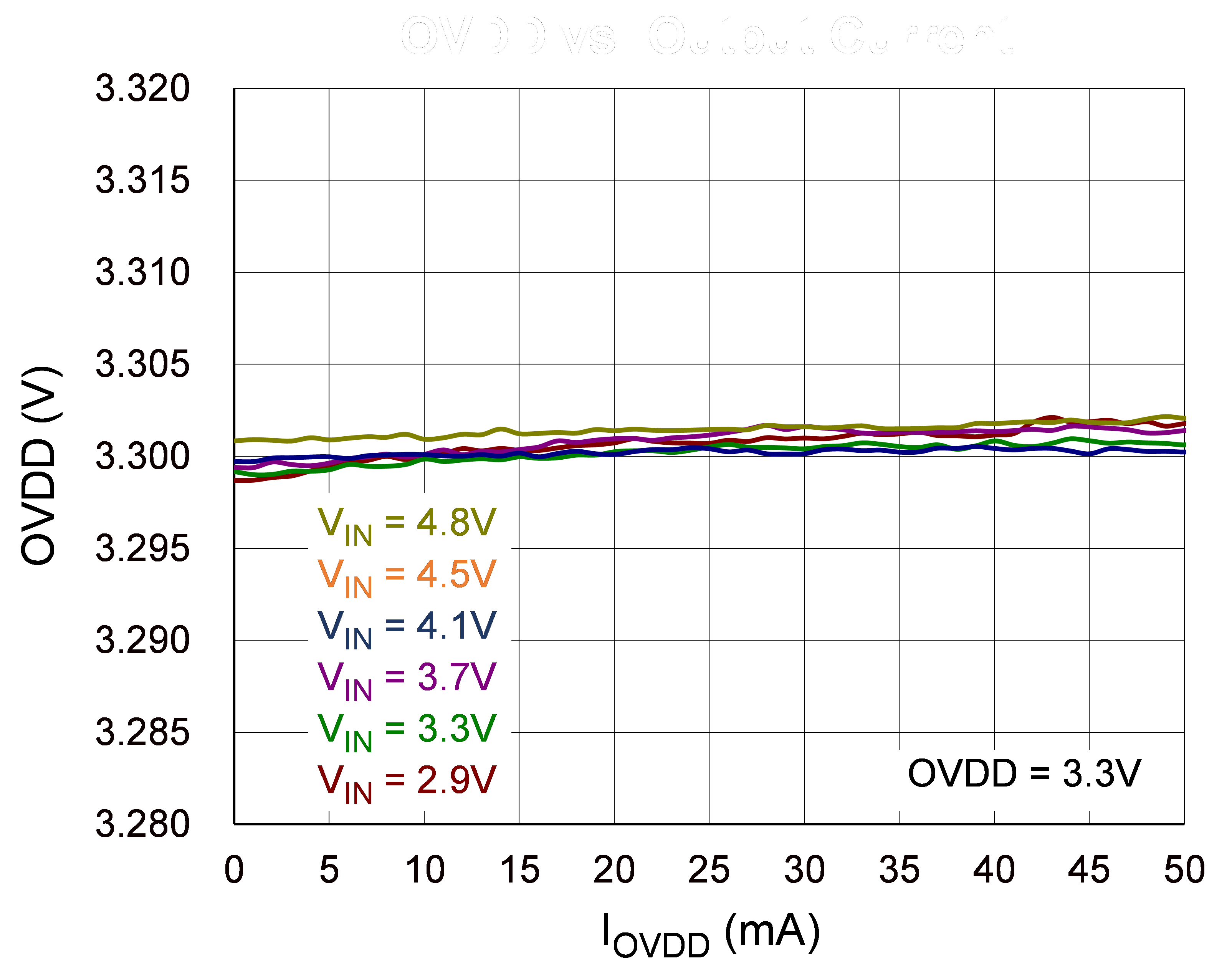
OVDD vs. Output Current
|
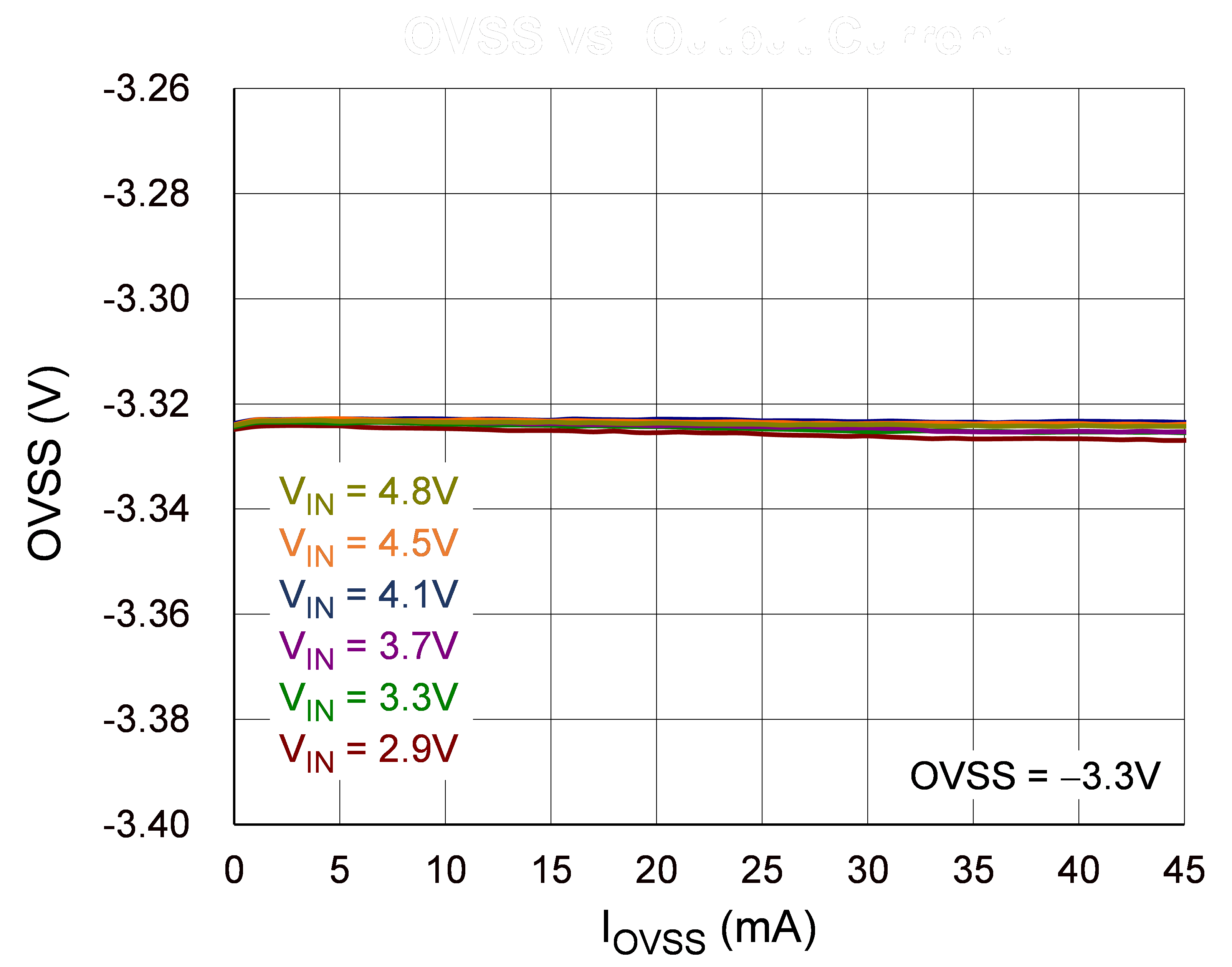
OVSS vs. Output Current
|
|
|
|
|
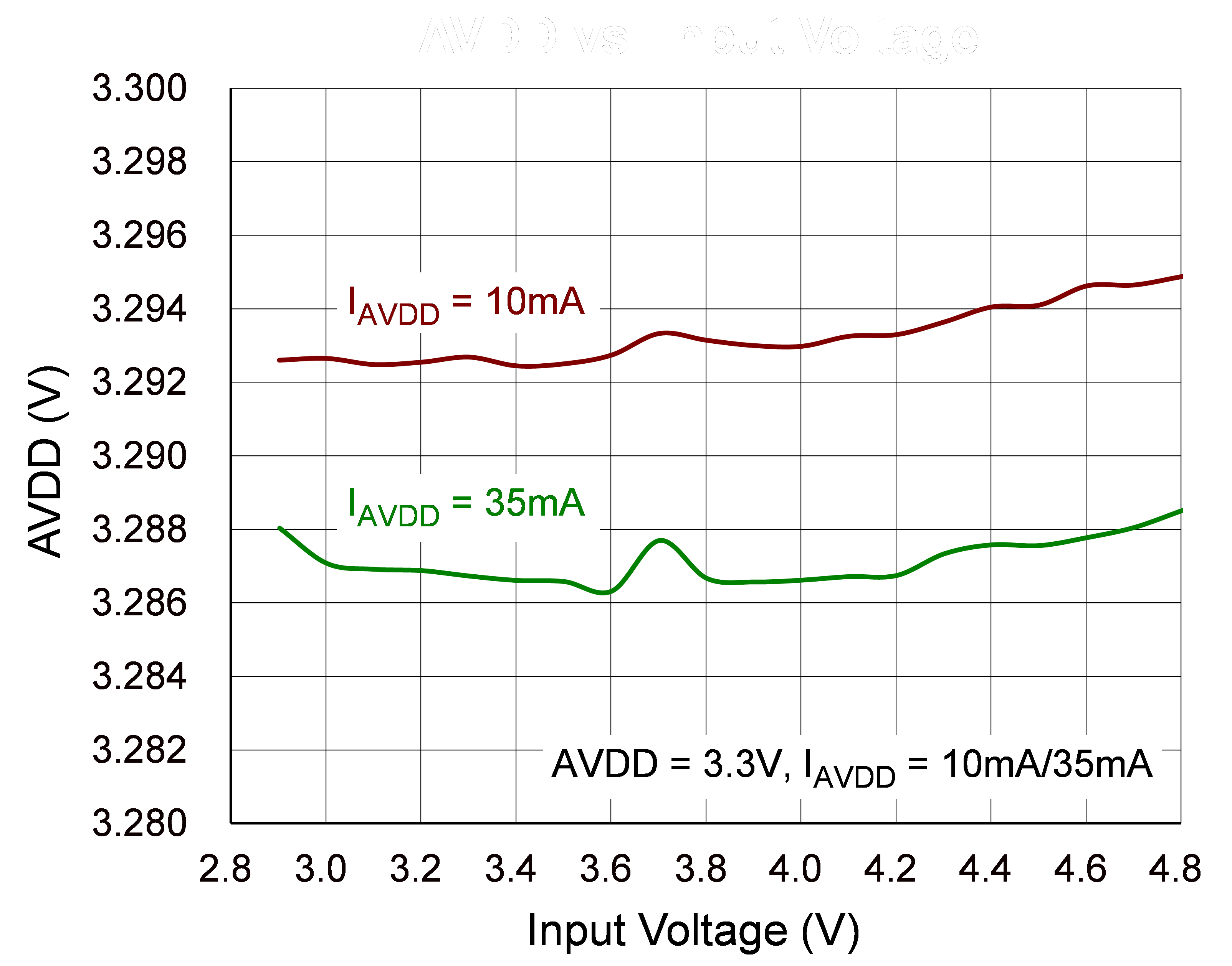
AVDD vs. Input Voltage
|
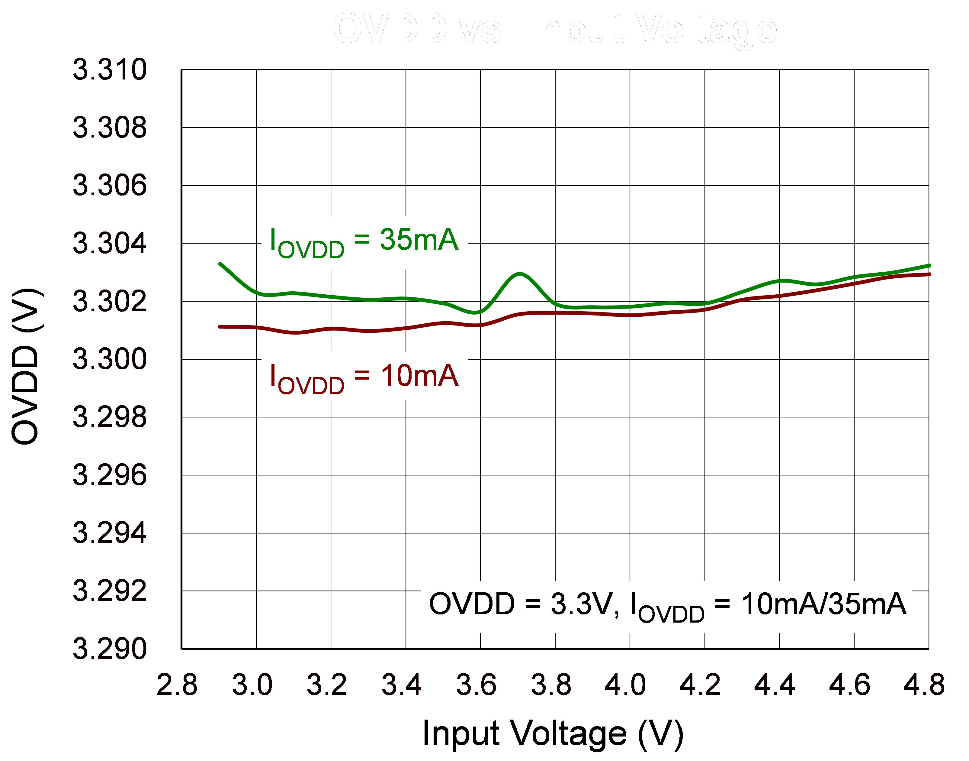
OVDD vs. Input Voltage
|
|
|
|
|
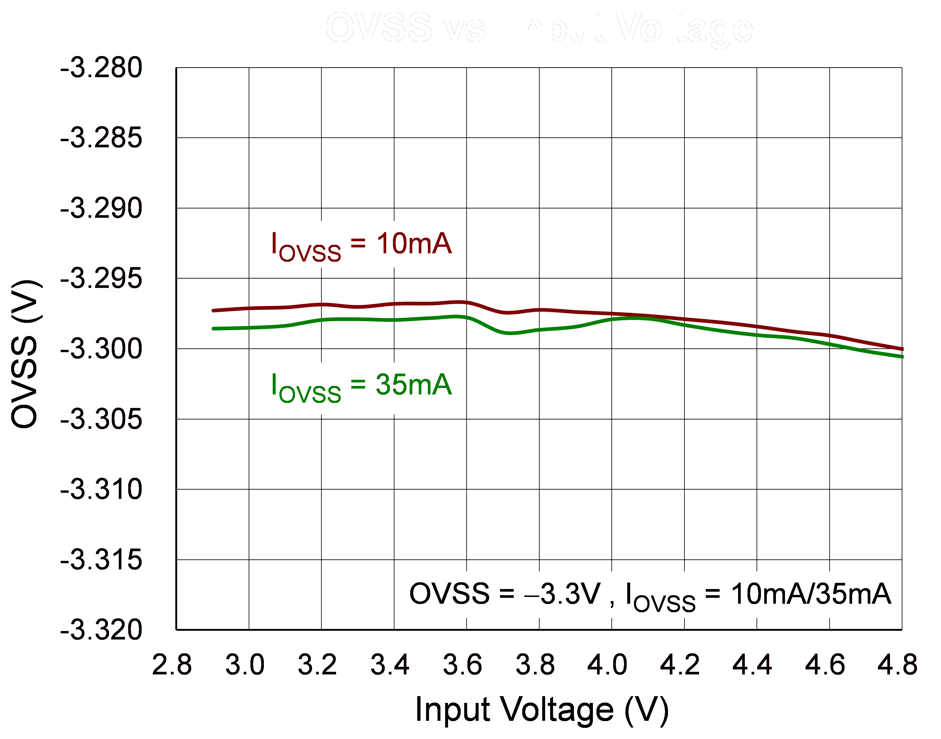
OVSS vs. Input Voltage
|
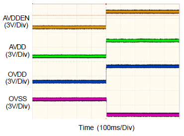
AVDDEN Power On
|
|
|
|
|
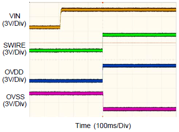
SWIRE Power On
|
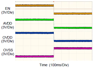
AVDDEN Power Off
|
|
|
|
|
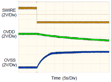
SWIRE Power Off
|
|
|
|
|
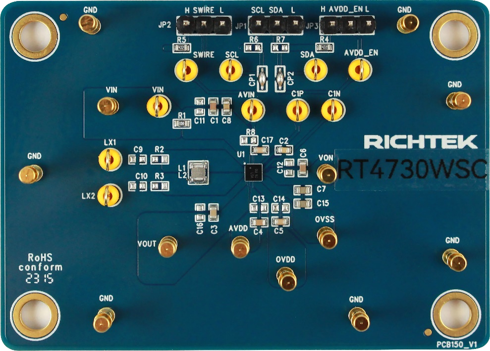
Evaluation Board Layout
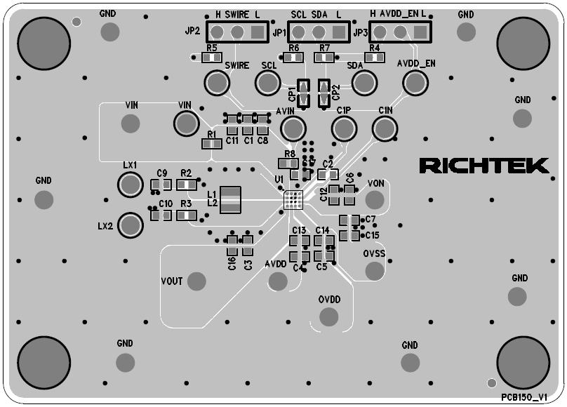
Figure 1. Top View (1st layer)
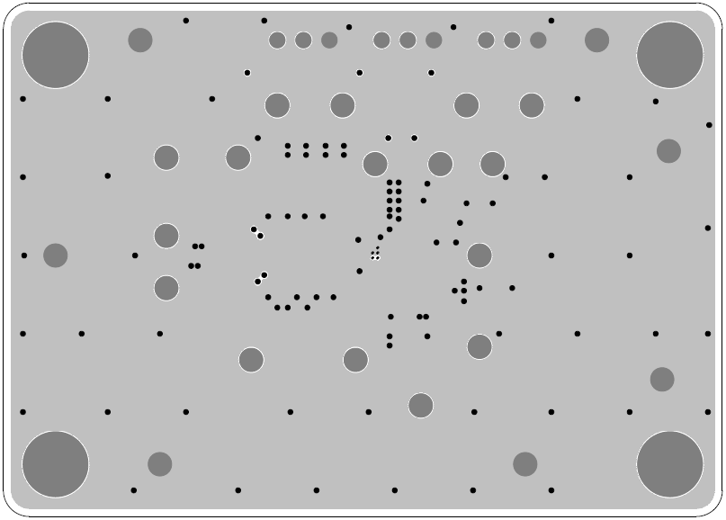
Figure 2. PCB Layout—Inner Side (2nd Layer)
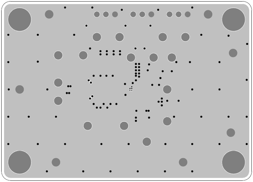
Figure 3. PCB Layout—Inner Side (3rd Layer)
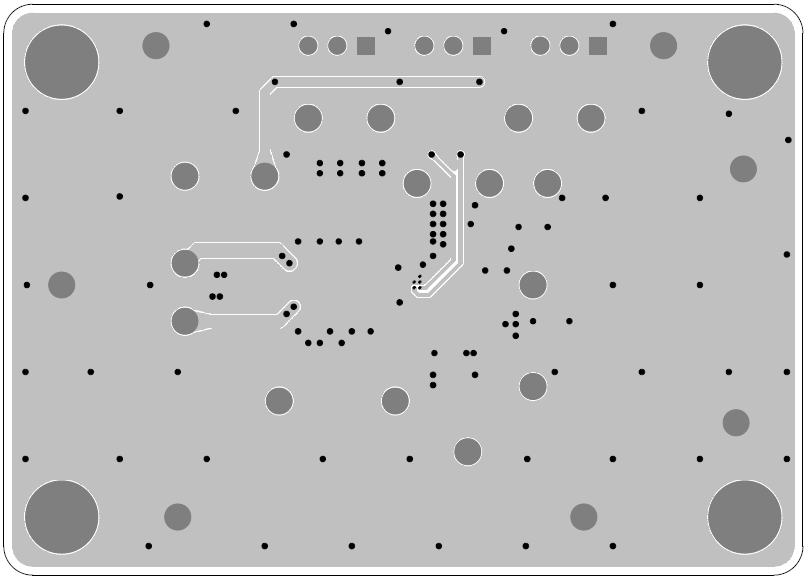
Figure 4. Bottom View (4th Layer)